
Semiconductors are the foundation of modern technology. These components power everything from the smartphone in your pocket to the advanced systems in electric vehicles and data centers. The manufacturing process begins with a silicon wafer. This is a thin, circular slice of semiconductor material used as the substrate for integrated circuits.
Because these wafers serve as the base for complex electronics, their structural integrity is important. Even a microscopic flaw can lead to the failure of thousands of individual chips. Traditional inspection methods often struggle to scale with mass production, creating a need for automated, high-precision solutions.
In this guide, we will explore how to use computer vision to automate semiconductor inspection, specifically focusing on identifying macro-scale physical defects on silicon wafers.
The Importance of Wafer Inspection
In the semiconductor industry, yield (the percentage of functional chips produced) is the primary metric of success. Physical defects like cracks, scratches, and surface contamination can occur at any stage of the fabrication process, causing lower yield.
While some defects are deep within the circuitry, many critical failures are from structural issues on the raw wafer itself. Automated object detection allows manufacturers to identify these "macro" defects early in the production line. This early intervention saves time and resources by preventing further processing of compromised materials.
Choosing the Right Vision Model
When building a vision system for semiconductors, the choice of model depends on the scale of the inspection. We have identified two primary directions for wafer analysis:
- Microscopic Analysis: Utilizing instance segmentation to identify chemical and mechanical flaws like block etch or contamination at the die level.
- Macroscopic Analysis: Utilizing object detection to identify large-scale physical defects such as cracks and scratches across the entire wafer surface.
For this project, we are focusing on the Macro View. This approach provides a good look at the physical wafer presence, ensuring that the structure/base is faultless before proceeding to more specific manufacturing steps.
If you prefer a visual walkthrough over the written steps, check out this video. It covers everything from cloning the dataset on Roboflow Universe to training your custom detection model:
Step 1: Access the Roboflow Platform
Begin by navigating to Roboflow and signing in. If you are new to the platform, you can sign up for free to get started immediately. Once inside, ensure you have a dedicated workspace organized for your computer vision projects.
Step 2: Acquire the Wafer Dataset
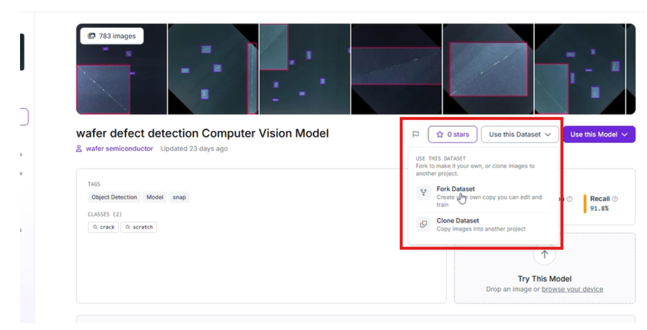
To train an effective model, you need a high-quality dataset. We are using the Wafer Defect Detection dataset available on Roboflow Universe.
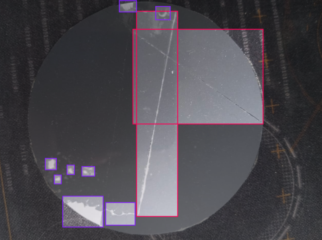
This dataset is specifically curated to help models recognize physical anomalies. It includes various examples of:
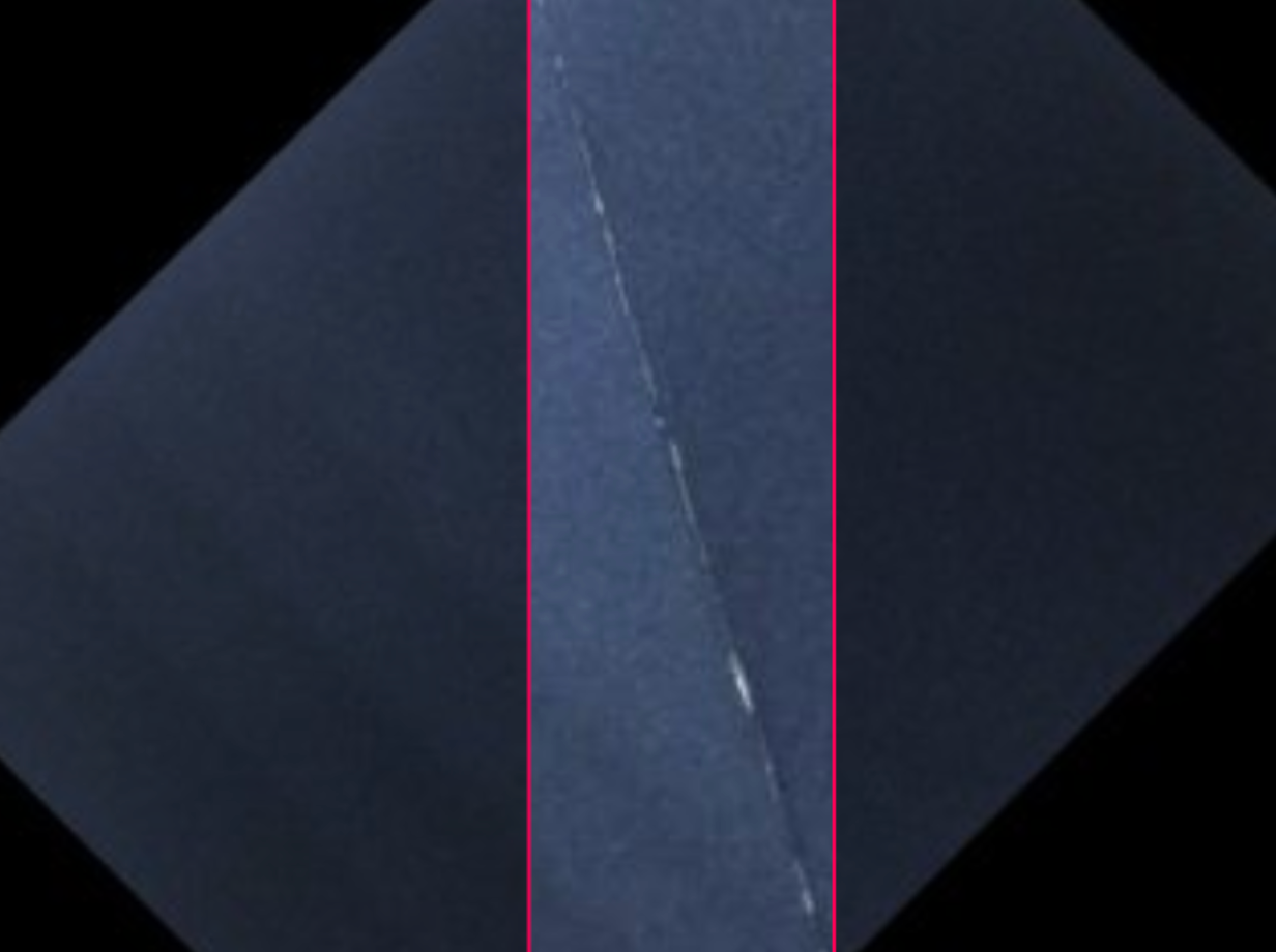
- Cracks: Structural fractures that can compromise the wafer's stability.
- Scratches: Surface-level abrasions that can disrupt the lithography process.
- Surface Defects: General anomalies that indicate a failure in the wafer preparation phase.
This model acts as the primary perception layer for your automated quality control system. To see how these models integrate into larger automation flows, explore our tutorial on vision agents.
Start by forking the Project: Select "Fork Project" to pull the images and existing annotations into your own workspace for further customization.
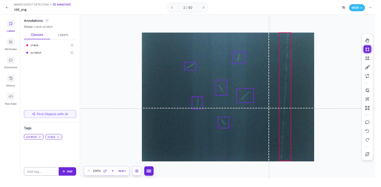
Step 3: Refine Your Annotations
To tailor the model to your specific production environment, you can add new images of your unique wafer types. Use Roboflow's labeling tools to draw bounding boxes around any identified defects. Ensure that labelling is always consistent. This can help the model learn the difference between a lighting reflection and a genuine crack.
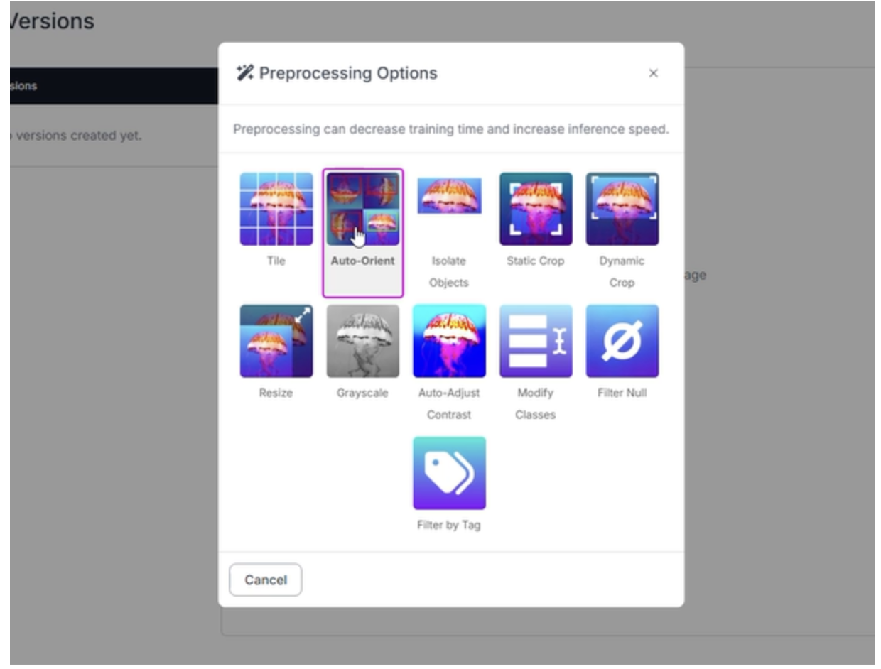
Step 4: Configure Preprocessing and Augmentation
Industrial environments are rarely perfect. Your model needs to be "hardware agnostic," performing reliably even if a camera is slightly out of focus or the factory floor lighting fluctuates. For this wafer project, we applied the following settings:
- Auto-Orient: Applied to ensure images are correctly rotated regardless of camera mounting.
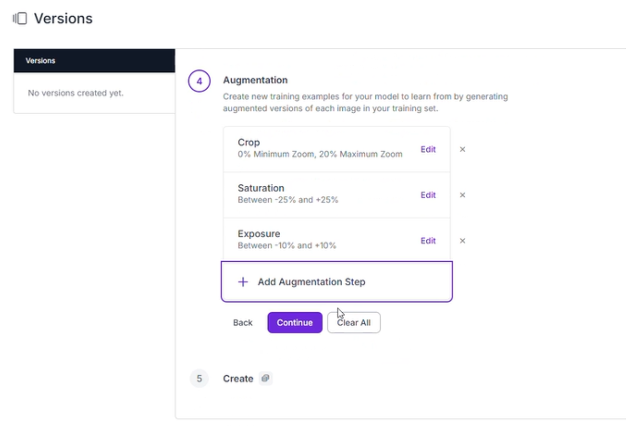
- Augmentations (Outputs per training example: 3):
- Crop: Between 0% Minimum Zoom and 20% Maximum Zoom to help the model identify defects at varying distances.
- Saturation: Between -25% and +25% to account for different wafer finishes.
- Exposure: Between -10% and +10% to simulate various lighting conditions on the line.
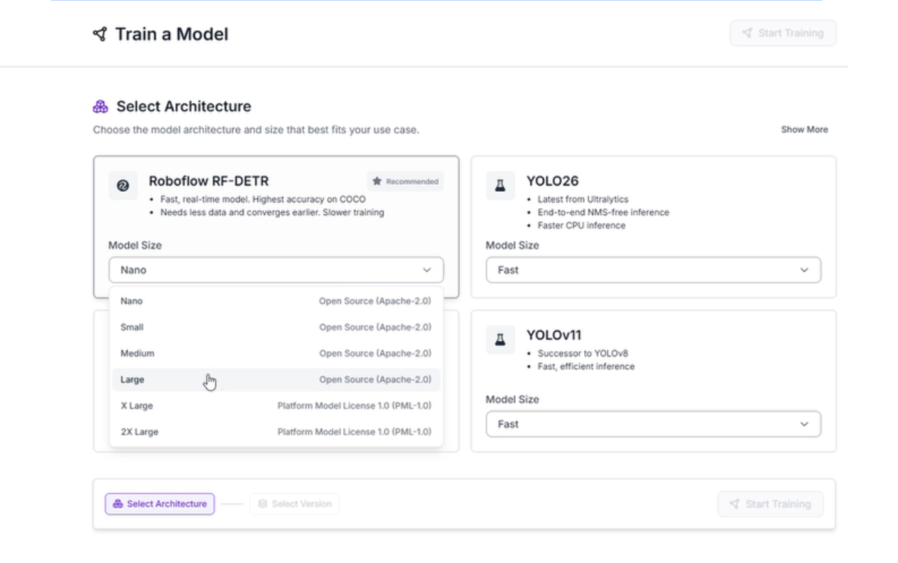
Step 5: Execute Training with RF-DETR
With your data prepared, it is time to train an RF-DETR (Roboflow Detection Transformer) model. This architecture is designed for precision, utilizing transformers to understand the global context of an image; perfect for spotting defects across the expansive surface of a silicon wafer.
- Launch Custom Training: Head to the "Train" tab and select "Train Model." This offloads the heavy lifting to Roboflow’s cloud-based GPUs.
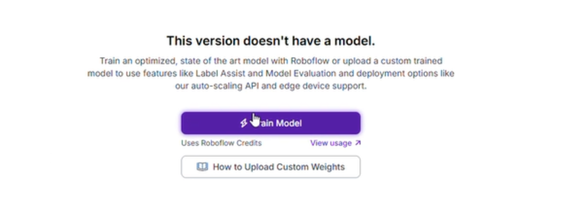
- Select Architecture: Choose the RF-DETR Medium model. This version provides the high accuracy and real-time performance necessary for semiconductor manufacturing.
Step 6: Evaluate Results and Model Performance
After training is complete, the Roboflow dashboard provides a deep dive into how well the model is performing.
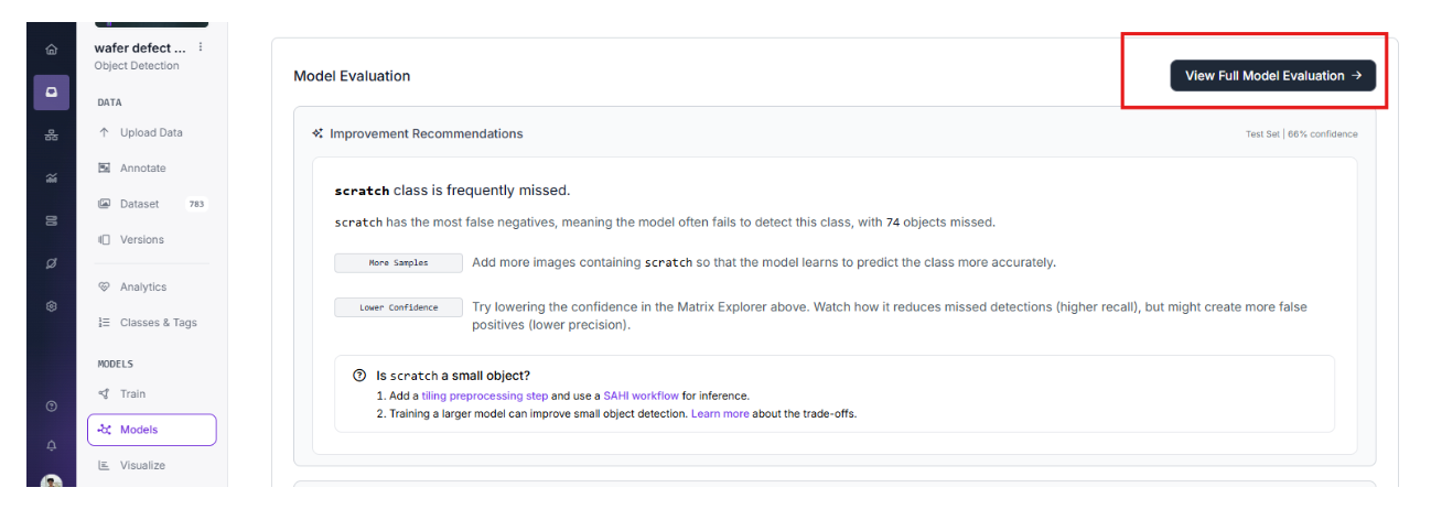
Our latest training run yielded impressive results:
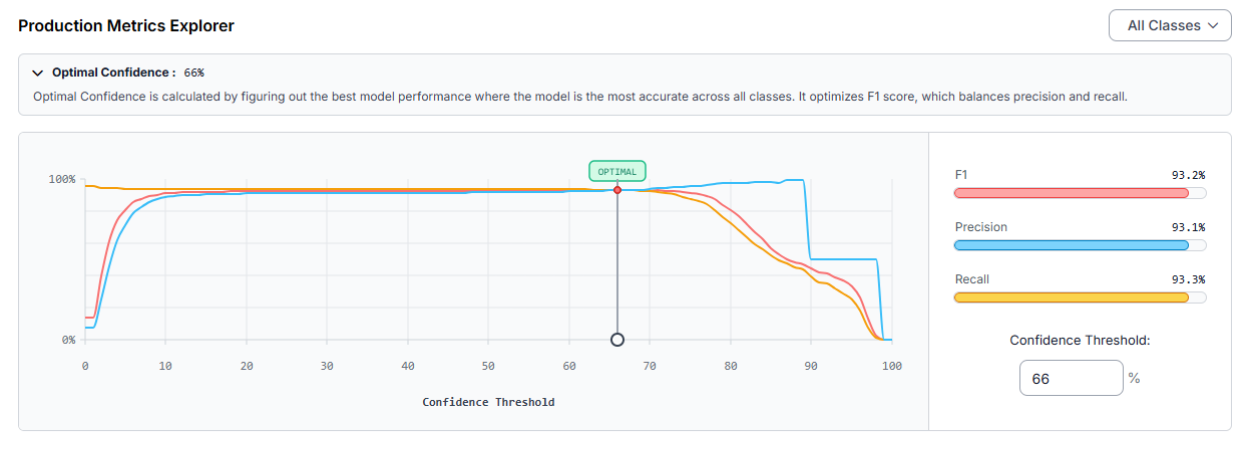
At an Optimal Confidence of 66%, the model demonstrates a strong balance between catching all defects and avoiding false alarms:
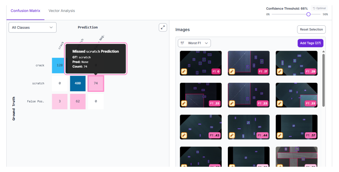
Identifying Opportunities for Improvement
By analyzing the Confusion Matrix and class-level performance, we can see exactly where the model needs more help. In this dataset, the "scratch" class is the primary source of false negatives. Specifically, 74 objects were missed during the test phase.
To improve the next iteration of the model, we can take the following steps:
- Add More Samples: Incorporate more images specifically containing scratches so the model learns their unique visual signatures more accurately.
- Implement SAHI: Because scratches are often small and thin, adding a tiling preprocessing step and utilizing a Sliced Aided Hyper Inference (SAHI) workflow can significantly improve detection for these tiny features.
- Confidence Tuning: Depending on the factory requirements, lowering the confidence threshold slightly can increase recall (missing fewer defects), though it may introduce more false positives.
By implementing this vision pipeline and continuously refining the model based on these performance metrics, you can automate the detection of structural flaws, ensuring that only perfect wafers move into the next phase of fabrication.
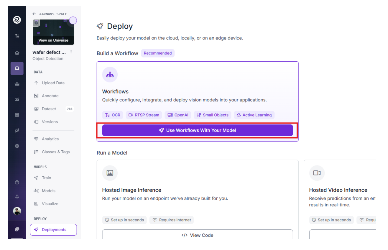
Step 7: Deploying the Solution with Roboflow Workflows
After training, the model can be deployed to the edge using several low-latency methods. For a manufacturing floor, deploying via a dedicated inference server ensures that data remains secure and inspection happens in real-time.
We can use Roboflow Workflows to build a complete application around this model. Simply click the "Use Workflows With Your Model" button in the deployment tab to create a custom pipeline.
After that, you can choose to use any template provided based on your personal/company preferences. For now, we can choose to build our own:
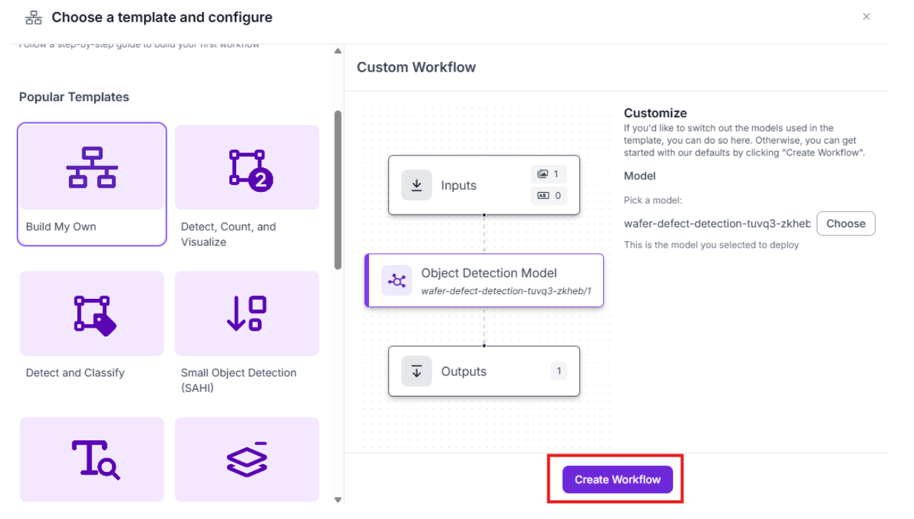
From there, within the Workflow, you have the flexibility to:
- Add a "Thinking Layer": Integrate an additional AI model or LLM to perform complex reasoning on the detection results.
- Automate Actions: Use built-in automation tools to trigger emails or system alerts the moment a defect is identified on a wafer.
While we are keeping the current deployment streamlined for maximum speed, adding a thinking layer is highly recommended for projects requiring extreme accuracy. You can learn more about this approach in our guide to vision agents.
Computer Vision for Semiconductor Inspection Conclusion
Computer vision is transforming the semiconductor industry by making inspection faster and more reliable. By focusing on macro-scale defects with models like those found in the Wafer Defect Detection project, companies can significantly improve their yields and reduce waste.
If you are ready to start building your own inspection system, you can sign up for a free Roboflow account to begin labeling and training your models today.
You might also be interested in learning more about small defect detection with computer vision.
Written by Aarnav Shah
Cite this Post
Use the following entry to cite this post in your research:
Contributing Writer. (Feb 24, 2026). Computer Vision for Semiconductor Inspection: Detecting Wafer Defects. Roboflow Blog: https://blog.roboflow.com/computer-vision-semiconductor-inspection/